Saturday, August 20, 2016

SMD reflow soldering


This is a overview of my SMD PCB assembly setup.

PCB

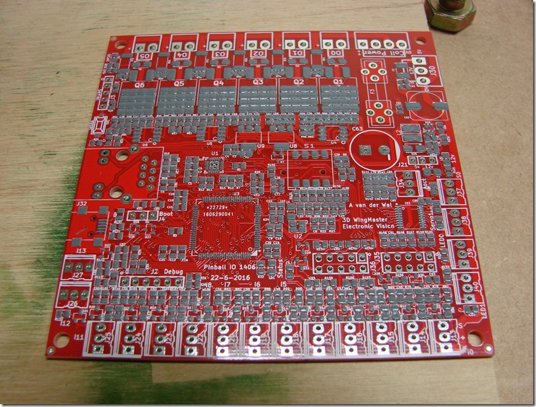
The PCBs and stencil have arrived back from DirtyPcb. Initial there was a problem with the gerber files I send them. This was caused that the manufacturer could not not process gerber header comments. After switching these off, the files where accepted.

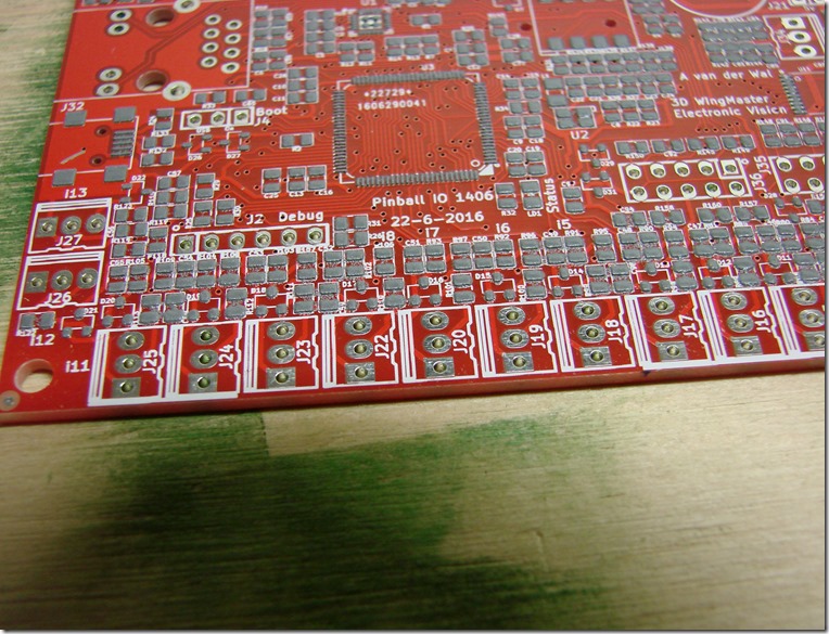
The PCBs are very nice. I was a bit nervous if the via could be made correctly, but those turned out to be no issue. For the via I used a drill size of 0.4mm and via size of 0.7mm. This leaves only a very small annular ring width of 0.15mm (about 6mill). That this is very close to the production limits of the vendor. Any errors in the drill to pad alignment would lead to disconnected via.

You order about 10PCBs. Due to the critical via’s I expected a bit less as 10, but received 12 of them. Nice! Most of the pads have small dimples in them. These are from the electrical test. In a machine two or more flying probes make contact to the various parts of the PCB, and check if the tracks are conducting and have no short to other tracks.

One of the PCB has some strange extra tracks on them. I assume they are cause by junk on the pcb during etching. But they did not seem to be connected to anything, so no real issue.

Interesting is that the manufacturer creates the stencil from the solder mask data not from the paste mask as you would expect. They did a nice job on it too.

DSC00516 - Crop

Paste application

Next challenge was putting the solder paste on the board. There are a couple rather small pads on the board from the QFN and QFP100 packages. So I needed a good alignment between the stencil and the PCB when applying the solder paste. For this I made a small jigg. The two empty PCB boards have the same thickness as the real PCB. They are mounted on a piece of wood, so that the real PCB fits very tight between them.

DSC00522

Then I taped the solder paste stencil in place. The stencil is not framed to save on freight cost. It has to be supported during paste application. The top and bottom of the stencill are supported, but sides of the stencil not. This did not seem to create any problems when applying the paste.

DSC00523


The solder paste used is leaded solder paste. I bought this 1.5 years ago and had stored it in the fridge. The paste has normally a limited self live, because the flux attacks the solder. After testing the paste on a small test board, it looks to still work good, so I went ahead with it. After reading about it, it seems the lead free solder has much shorter shelf live as lead solder. The flux used in lead free is more aggressive and reacts more with the solder as the leaded variant.

I ordered lead solder, because it melts at a lower temperature as lead free. Lead solder melts around 200 degree and lead free around 250.  This is so much closer to the breakdown temperature of the epoxy PCB material, making the reflow solder part is more critical.

The solder paste is first mixed very good and then applied to the bottom of the stencil. I applied the paste with a putty knife of 10cm wide. This worked quite well, but the putty knife was just not wide enough to apply the paste in one go to cover the 10cm wide PCB. On the right side I had to apply it twice. This brought too much paste on that side, but lucky caused no issues during reflow. Next time I will try a stainless steel dough cutter that is much wider. (oops, my wife saw it and was reassigned a new purpose…)

DSC00532

Even with the multiple solder paste application, the deposed paste look very good. I has very happy about that. Applying the paste with a stencil seems to be a very forgiving process. Most of the paste was applied in 2 strokes. The paste was put on the ‘bottom’ side of the mask.The first stroke upwards with little pressure to spread out the solder paste over the board. The second wipe with much more pressure goes  downwards from top to bottom to fill the holes and scrape of the excess paste off. All the excess paste was put back in the box.

After carefully lifting the stencil a very nice paste pattern showed up. DSC00517

Not bad at all for my first ever solder paste application! Surprising crisp edges of the paste.

DSC00519

Component placement

Now the fun part. Placing all these 100 tiny components. I mainly used 0805 parts, so they where no too small.

To help with placement, I marked a component printout with colors indicating the value of the part.  One sheet for the resistors and one for the capacitors needed.

DSC00544

The SMD components I store in envelops in shoe boxes. This creates a very compact storage for a large number of parts. Every envelope I mark some basic information what it is and where is was ordered from.

Most of the parts are ordered through Aliexpress. So much cheaper then distributors like Element14, but you need to wait a bit longer on for the order to arrive.

IMG_20160619_123518

Envelops in shoeboxes are great for storage of the smd parts, but for applying the parts they need to be easier accessible. All the parts that are needed on the pcb in the largest quantities where stuck on a bit of wood with double sided tape. This worked very good. The tape was pulled off easy without letting the parts fly everywhere. I marked the tapes with the same colors as on the placement drawing.

DSC00533

To place the parts I build a vacuum picker from parts laying around.The vacuum pump is a modified air pump (source unknown). I added a tube to the inlet of the pump. A small adjustable voltage regulator (2 transistors and a potmeter) is used to control the speed of the pump.  The pump creates a pulsing vacuum, but that does not seem to matter at all.

I adjusted the pump speed such, that it just picked up the largest parts needed. Even on low speeds it can still pick up a whole qfp100 package on a tiny needle.

DSC00534

In case a small component was sucked in, I added a film canister to capture them. (that was the last film canister, not all obsolete and now unobtainable). In hindsight quite unnecessary. The vacuum picker needle is too small to suck them in.

DSC00536


This is the vacuum picker. It is made from a 10 ml syringe. The tip is a standard luewer blunt needle available all over aliexpress. The plunger was cut and drilled so the red hose could be pushed through. The handles on top of the syringe where cut off.

A small hole is drilled in the side of the syringe. Keep it closed with a finger when picking parts up, and opening it to release the part. After placing 10 parts, I found out that you just can keep the the hole closed when placing the smd part in the solder paste. The paste is so sticky that is holds the part better as the picker. So the hole was taped closed. This also helped a lot to orientate the parts, because you don’t need to keep the hole covered. Sometimes the part need to rotate 90 degree or more. If you don’t need to hold the hole close you can roll the syringe between your fingers. An alternative you can also re-orientate the SMD holder, so you don’t need to rotate the syringe. I tried that too, but rotating the syringe is easier and faster.

The red tube is silicon tube. It is very flexible so does not hinders movement.

DSC00531 - Copy


It did took me about 2.5 hours pick and place all the SMD parts. The 3 pin sot23 are surprising difficult to place. The solder pads are small, and the device has only one correct orientation. I noticed that in the end after about 3 hours the tackiness of the paste had reduced a lot.   I still need to make at least  4 more PCBs, so I hope the next PCB will go faster.

The last parts placed where the QFN and QFP packages.Needed a sturdy hand when placing them!

DSC00520


Reflow soldering

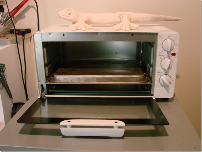
I came across several types of reflow soldering approaches:  Skillet, hot clothes iron, dedicated reflow machines and toaster ovens. I was tempted to order a dedicated reflow machine from Aliexpress, till I came across a very cheap toaster oven at the local KMarkt. ( I had to confiscate it back from kitchen duty)

Reflow soldering needs a certain time / temperature profile. In general you should not rise the temperature to fast, otherwise this can cause stresses and cracks in the components. Also you need to hold the temperature steady around 150 degree during 2 minutes to allow for preheating the board and components. After the preheat follows the soldering. The board is heated to 210 degree for 20 sec. with at least 60 sec above 180 to activate the flux.

I experimented a bit how to get close to this solder profile, and came to the following sequence:

- turn oven on (all elements, oven temperature setting on maximum so that it does not cut out)
- oven off when temperature reaches 120 degreeC. The temperature will rise further to about 150 degree
- after 2 min at 150 degree switch heater on again.
- turn heater of at around 210 degree.
- wait 20 sec
- open door partially
- wait  to cooled of below 150 degreeC then open door fully.

It is very interesting to see that all solder paste suddenly goes from mattisch grey to shiny silver solder around 195 degree.

During one test I liked to see how hot the oven could get. I had a small empty PCB in the oven. When the oven reached 300 degree, the PCB started to smoke and smoke. It cost 3 weeks before the awful burned PCB smell was disappeared :-<  I was surprised that the epoxy PCB could not tolerate that temperature. Lesson learned : no more heating  of pcb to 300 degreeC. Still a bit worrisome that for lead free solder the solder profile reaches 250 degree. Quite close to the 300 disintegration temperature.

A very sad lizard with a broken leg is sitting on a warm spot, waiting for the doctor.

DSC00543

To measure the temperature I used a thermocouple temperature meter. The probe rest on the metal plate close to the PCB. It is winter at the moment in New Zealand, so it was a bit chilly in my hobby room.

DSC00539

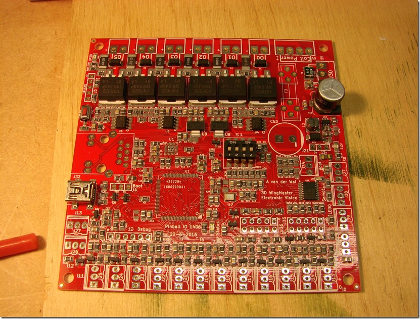
The PCB came out very nice out of the reflow process. I only needed to fix some shorts between the QFP100 package. That one was off halve a pin distance when it was placed in the solder paste, and needed to re-centered on the pads. That caused some solder paste mess that the reflow had not fixed fully..

Added all the through hole connectors, except the RJ45.

DSC00542 - Copy

Al in all, I am really happy with the end result. It almost look factory made.  Now I hope it all works.

Testing

The DC DC converter creates a nice 11.5v as calculated from 5v rail. The input channels work on 12v and 5v.

Currently still setting up the software build environment to use for CPU testing. Next test is the CPU, power driver and finally the Ethernet.
Wednesday, June 29, 2016

Pinball electronics II


Finally finished the PCB design of the pinball IO board. It did cost me more time as expected to squeeze all the tracks on the board.  I  just send the design to  Dirty PCBs to be manufactured. 

The pinball IO board primarily function is to control coils and LEDS, and the read sensors and switch. Likely for the firepower pinball, I also use the board as a central controller. That machine does not have a DMD or matrix led display, so the board would be sufficient. Alternatively a Raspberry-pi as master controller is also still a good option.

Board

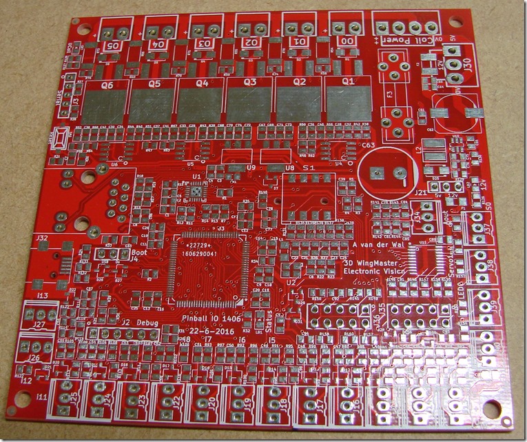
Below you can see the final pcb. It is a double sided board with a mix of SMD and through hole parts. All components are mounted on top side, except one. The surface mounted micro-sd connector has to be placed on the bottom side due to lack of space on top.

The pcb ended up as 10x10cm (4x4inch). This is a standard and cost effective size of PCB available at a lot of Chinese vendors. Most resistors and capacitors are 0805 size. I choose 0805, because I had already a set of these at home, and they are still good size to handle. Possible in hindsight I should have used 0603 instead of the 0805 to save some space.

All connectors are through hole. These are stronger and more cost effective then surface mount versions.

image

The picture shows the top silkscreen and top traces. Both the top and bottom copper layers are very crowded around the U3, the 100pin processor. On the end had a hard time squeezing the last traces in.

The most critical component on the pcb is U1: the QFN package of the LAN8720 Ethernet phy. I ready hope I manage to solder the fine pitch QFN part with all its hidden pads to the board

Originally I planned to have 8 coil outputs and 16 digital inputs. But that did not fit on the 10x10cm pcb and had to drop some. The PCB ended up having 6 coil drivers and 14 switch/sensor inputs. This is still very good ratio. For a Firepower pinball you only need 4 or 5 PCBs, depending if the master can handle coils or not.

In some way I always end up with boards that have to many features. Also this board. If I would have limited the board features to only coil outputs and sensor inputs, the routing of the board would have been so much easier. But no, I like to put more features on it. And a lot of times never use all these extra features…..

Features

I will never learn. So the board ended up with the following features:

- A 100baseT Ethernet interface. The primarily control interface
- A mini usb connector. This can be used to programming and control.
- A micro-sd card connector. Used to store log files and music and other data.
- 6 outputs with  high voltage (upto 50v) & high current outputs for coil and motor.
- 14 digital inputs. They can supply either a 5v or 12v rail to feed the sensors.
- 2 analog outputs for either audio or other controllable voltages.
- 2 LED chain outputs controlling a row of programmable WS2812 RGB leds.
- 2 Servo outputs
- a 5v and a 3.3v digital IO connector supporting various interfaces type like I2C, UART, SPI and general IO.
- a voltage boost from 5v to 12v.
- a ARM Debug header
- Uart interface for debug or other purposes.
- A 4 bit dip switch to set the Node address.
- buffer capacitors on the high voltage and 5v rails.
- Glass fuse in the high voltage (0..50v) rail . Poly fuse in the 5v rail and sensor power rail.
- Couple of power rail and status leds.
- And a very usefull reset button.


CPU

The CPU choice has not changed. I am still using the STM32F407VGT6 . Originally I planned to make a excel sheet to select the pin usage of the processor. But then I came across the program STM32CubeMX from ST. Very useful. This program allows the selection of peripherals you like to use. It right away marks other interfaces that are not accessible any more, because the pin is in use. So it is a bit of trying out till you have the correct combinations.

image

And also very nice is that is can create all the header files needed to initialise the CPU. This even inclues FAT filesystems, TCP/IP stacks and even FreeRTOS.  I still have to try out this part.

Coil drivers

The coil/motor outputs are capable of a lot of amps and volts. The IRF3710ZS Fets are good for 100v and 59A. Current limiting factor will be the PCB tracks and fuse rating.  A glass fuse protects the board and coil from overheating. The voltage is limited by the 63v elco used as buffer, and the track to track spacing on the PCB.

Each coil current is measured by the processor, so the CPU can disable the outputs on a high current.  I also going to try if a controlled output current is possible. In that case instead setting a PWM percentage like all other boards, you can set the coil current. Coil current has a direct relation to coil power and heating.

The fets are driven in saturation by a gate buffer chip IR4427S. In that way the heating of the fets will be minimised. To drive the the fets in saturation a gate voltage >8v is needed.

PSU

Originally I have planned a 12v input voltage, and step that voltage down to 5v and 3.3v for the led and logic. Sadly the inductors needed are quite large to create the 2 to 3 ampere needed on the 5v rail to feed all the ws2812 leds.

Therefore now the board is fed with 5v and a boost converter is used to create a 12v rail. The 12v is used to the FET drivers and optionally to feed the input sensors. The sensor can also be feed directly from the 5v rail, jumper selectable.

The 5v is directly fed to the leds and servos, after passing a poly fuse and buffer capacitor. With two AMS1117-3.3V linear regulators the 3.3v rails for the PHY and CPU are generated.  I used 2 because the exact current needed by the Ethernet phy and CPU was quite uncertain .

Some parts


 image

Mini-USB. I liked to have micro-usb, but could not find a nice SMD version.

image

Micro SD connector. This is a push/pull version

Schematic/ PCB design

I used Kicad as cad tool. I was very very pleasant surprised that Kicad was working so well. I uncounted hardly any problems with the program. It was very stable and usable. Lot of people complain about the user interface and library management, but that was not my experience at all. You have to set up the libraries you like to use, and need to lean the key presses. But thats it.  I also use Altium quite a lot for PCB design. Altium has much more features, but if you look what you actually need and use, then kicad is just as good! In kicad to tend to need less keypresses as in Altium for most functions. E.g. start a new track is the most used function during PCB design. In altium this is p t (2 keypressses)  in kicad x (1 press). After a day work that saves you 100’s or even 1000’s of presses.  Altium is around usd$7000? per user, and Kicad is free without limits. Kicad is now so mature, i don’t see any need for expensive programs like Altium or Eagle. 

As a base set of symbols and footprint i used http://smisioto.no-ip.org/elettronica/kicad/kicad-en.htm a lot. Also very nice is the integration with git. This allows to load footprints from a central GIT repository! Very nice. In the end I had copied most footprints to my own library. In a lot of cases the silkscreen is over the pads what is not very useful. Also a lot of  pads are minimal in size that I liked larger for a more robust design.

The only thing that does not work yet in my setup is the 3d view. I have not figured out what path to set. But I did not miss the 3d view to much. In Altium this is also more a gimic. The primary use of 3d I think it to be able to save a 3d model of the pcb. That model then can be loaded in a 3d design program to check if it fits in the housing.

Some things are a bit strange in kicad:  For example in the PCB program has different canvas : F9 and F11 and even F12 (never used F12), that each has its own set of features and menu’s.  Caught me out a few times. Also there are a lot of buttons on the screen that you never need to use, and could be removed to have more space for the PCB itself.

To position parts, I used F9. If you select a part in the schematic, it is highlighted in the PB and other way around. This help very much in placement . All the track wrok I did in F11, because that has much better track colouring and of course the track pushing option.

For quite a while I did not know it that the kicad version I used had a push and shovel router! That is only available in F11 and when you enable it in the menu. Should be default on. But that is a very powerful option to get an extra track in a tight space. It has some unpolished aspects, like breaking tracks into many segments if going around a pad. But lucky it cleans up a lot of that if you push nearby track a bit!

In the PCB program I mainly use the following keys:

- x lay a track
- v  add via or swap layer
- e  edit part or router setting
- delete   a track
- w and shift w   to change track width.  (I should change this this w and q)

I still need to find a way to change grid spacing with key presses.

I use a 10mill grid to place parts, and 1 mill grid for tracks.  Track widths used are 0.25mm 0.5mm 1mm 1.5mm and 2mm

Board population

Besides the nasty QFN part has the board lots and lots of other parts. It will be fun  to load up the board with this massive amount of passives.  Now I have to be careful. I am reading way to many web sites about pick and place machines, and they look quite easy to make. Do not start another project….

To help with solder paste placement, I also ordered in a stencil at the same Dirtypcb manufacturer. To solder the pcb i bought a small toaster oven. Sadly my wife saw it and confiscated the oven for the kitchen duty  :-<

Also also looked into making my own stencils out of aluminum cans (see http://www.popsci.com/article/diy/build-diy-soldering-stencil-out-soda-can ) , and that does not look too complex. But not this time. I need to reduce the number of uncertainties to make progress. The number of uncertainties/first times is already way to high (kicad smd design, arm processor, arm toolchains, qfn packages, paste and refow soldering, 50mhz clocks, freertos etc etc)

PCB vendors

To find a PCB vendor with a good price the website http://pcbshopper.com/ is very useful. This searches with your given pcb specifications several vendors for pricing.


Now waiting for the pcbs to come back….

Sunday, March 13, 2016

Pinball electronics


I finally started on the hardware design. This will make it easer to start testing playfield parts.

The pinball will be driven by the following parts:

- A custom designed pinball IO board. This controls 8 coils and reads 16 inputs.It can control 2 led chains.  It is connected with an 100baseT Ethernet port. A firepower based pinball will use 3 or 4 boards, depending on design.

- A Raspberry Pie as central pinball controller. Alternative the custom IO board can play the pinball controller.

- Ethernet switch to connect it all.

- A 12V power supply to feed the LEDs and electronics

- A 24v or 48v  power supply for the coils.

- 7 segments units for score and ball counters.

Except for the IO board are all other of the shelf parts.

The first version will have simple 7 segment number displays for scores. Later on I like to add a LED matrix display.


Pinball IO controller

The pinball controller will have the following interfaces:

- 100 BaseT Ethernet interface

- 8x high current coil driver outputs with overcurrent protection.

- 16 inputs, working both at 5v and 12v

- 2x ws2812B led chain outputs

- Some digital IO to control stepper motor driver or other electronics.

- 2x servo outputs.

- Cpu program header.

- power connectors.

- if PCB space allows: 2 analog outputs

- Also pcb space depending : mini usb-b connector and micro Sd card connector.

To feed the ws2812b LEDs the IO board will need to have a switch mode power supply to generate 5v from 12v. The board will have a glass fuse for the coil , and PTC fuses for the rest.

The board is quite generic, and can be used for other purposes besides driving a pinball machine.

Design choices

CPU

There are not many low end ARM processors that have an Ethernet interface.  Initially the NXP LPC1759  was a good candidate, but it already some years old.  The ST  STM32F407VGT6  is a more modern chip with more ram and faster cpu. The 100QFP package has enough IO pins, so can interface with all the IO’s directly.

The issue is that all the IO pins of the CPU have about 5 functions. So it will be a puzzle how to connect them up.

Because of the Ethernet phy clock requirement, the cpu has to run on 25Mhz.  To reduce any risk I selected a crystal oscillator for this. They are the size of a grain of salt in:3225metric or 3mm long and 2mm wide.

Ethernet PHY

I was searching for an Ethernet phy with a PLL. It seems that the only types available all have a QFN package. This leadless package is a bit tricky to use. Even worse it has an exposed pad that also need soldering.  You really need to  work with a paste stencil and reflow oven to use them. Settled for a LAN8720 .  Both mechanical as electrical. IT is supplied with 25,hz from the CPU, and the phy PLL creates the 50mhz needed for the RMII interface. This part will be the most critical part of the whole design.

The rj45 connector has an integrated common mode coil and transformer.

PSU

Used here a super standard switch mode chip: LM2596S-ADJ. This device is used on 1000’s of designs. It will create 5v at max 3A. The 3.3v rails for cpu and phy are using a LM1117 LDO linear regulator from 5v rail.

Coil driver

Tons of fet available for this. Selected the same transistor as used the Medieval Madness Remade (MMR) electronics only in SMD version: the IRF3710ZS. These N channel Fets have impressive characterises for their price: 100V rating at 59A with a resistance of 18mohm.  You can get lower resistance versions, but the price rises. Also the transistor is not switched on all the time. At 10A continues they only dissipate 1.8watt.

The n channel fet needs to be driven to saturation. To do this the gate has to be above 8v. A dedicated driver is easier to use, and I selected a dual channel low end driver IR4427S. This so8 device can drive 2 fets, so there will be 4 present to drive the 8 fets.

A 0.01 resistor is used to sense the current through the transistor, monitored by the CPU.

Connectors

For all low current connections the family of Kf2510 connectors is used. A 3 pins version for each of the digital switch input. This connectors has a latch function that prevents the connector falling out. Sadly it is a through hole part, so can’t be reflow soldered.

For the higher current connections the family of  Vh3.96 connectors is selected. also these are lockable. The coil outputs are 2 pins.

Sourcing

Most parts are sourced from Aliexpress. I really hope that there will be no fake chips send, particularly for the CPU.

PCB

I am using Kicad as PCB design tool. A very nice tool with extensive PCB footprint library. Sadly the BOM part of the program is not implemented very will, but no complains. It is free.

A common and thus cost effective size for the PCB is 10 by 10 cm for double sided board. I would have preferred a longer and smaller board, but that would increase the costs a quite lot. To much for a prototype.

On this moment still drawing the schematics and need to finalise the cpu pin selection.

Saturday, March 12, 2016

Playfield construction


What would be the best way to make a playfield? There are so many ways to do this.

Playfield constructions

In general there seems to be two approaches

  1. Plywood with print on top and a thin protective coating op top. Inserts are glued in the playfield for lights
  2. Plywood or mdf with thick plastic plastic sheet that is printed on the back.

Opt. 1) plywood with inserts and coating

Approach 1) plywood with inserts and coating is the most common way to make playfields.

The playfield is first drilled/milled. Then the inserts are all glued in and everything is sanded, sealed and printed. Finally it is covered with some car grade clear top coat. 

Topcoats

The biggest issues for a DIY using 2 component clearcoat are that this stuff is poisonous, so you need a spraying boot with good dust masks etc. Also you need a good sprayer and compressor. And there is lot of sanding involved between every clearcoat layer. But this can be outsourced to a car painter.

An alternative clearcoat approach for DIY is using self leveling compound. This is normally used by artist to make there artworks shiny. This can applied in a single thick coat. Because it is self leveling property it creates a very smooth surface. For this you don’t seed sprayboots or sprayers so it done with less investments. I know one diy that has used this on his playfield successfully, but have not seen reports how good this holds up.

A other diy only way is to cover the whole playfield with mylar or thin polyester sheet.

Prints

The prints can be done in various ways:

- Silkscreen printing. This is the main way playfield where made in the past. You need to make a lot of silkscreens: one for every color printed.

- Direct print on wood/plastic with dye’s. This seems to be the common way most playfield are produced nowadays. For DIY is this also nowadays a usable approach, because the dye printers are quite common now. If the dye printer can not print white, the playfield first has to be sprayed white. Any insert need to be masked to prevent it being painted.

- Vinyl overlay glued on wood/plastic substrate. Typical only used for the outside of a pinball cabinet. Some people have used this approach also for there one diy playfields.

- Paper poster glued down: have not see anyone using this way.

- Decals: Typical only used for small area’s like inserts or small repairs. Possible worth a try if you can cover larger area’s without distorting the very thin decal


Opt. 2) Playfield with thick plastic sheet

The playfield with thick plastic is only used in a couple of pinball machines For example it is used in Elektra, Bushido, Canasta.

The playfield looks like this:

clip_image001

(picture from pinside user Star_Grazer)

The wood is either plywood or MDF.  MDF is more difficult to screw in, but it surfaces are normally very smooth. The wood has only holes, and maybe a sealer, but not other paints.

The plastic sheet has the graphics on the bottom/reverse side, so the graphics are fully protect against damage. The surface of the plastic is fully smooth, so no sanding or coating is needed. Likey a wax coat can be used to protect  the plastic better against scratches.

No inserts need to be glued. The shape the hole in the wood defines the insert outline. So this gies a huge flexibility and allows to choose any ‘insert’ shape and size as you like. There will likely be light bleed from the hole to the surrounding playfield. The bleeding can be reduced by making wide black area’s around the “inserts”.

Because you need to have access to a cnc to mill the wood, the plastic sheets can also be milled on the same machine . Instead a cnc a laser cutter can also be used. A laser cutter has the advantage that it create much nicer edges  in the plastic then what a mill can make, but cannot cut all types of plastic. If you have a powerfull enough lasercutter, you could even cut the wooden playfield with it. Any charring on the wood in fine and not visible. Because the holes are black, it is possible that that even helps reducing light bleed.

I looked around , but I could not find information on the web what the actual thicknesses used for the wood and plastics. If standard pinball mechs are used, then the total thickness of both wood and plastic need to be 1/2 inch or about 12mm.  Thus you could use 9mm wood and 3mm plastic.  If the thickness is less critical, then use of 12mm ply or mdf with 3mm plastic to make a stiffer playfield.

The type of plastic. This is also unclear what the excising machines are using for this. The most likely options are:

-  Plexiglass (PMMA, acrylic glass). This is very transparent and reasonable stiff material.

- PETG is a more flexible material. Lot of times used for transparent playfield parts and ramps.

- Polycarbonate. This is the strongest material (and the most expensive). Can not be lasercut due to poisonous vapours escaping. It scratches easy. 

print

The print can use the same approaches as for the plywood print. If the decal or vinyl approach is used, then these need to have holes cut in the same places as the plastic sheet to pass though any pinball mechs.

After the colors & black are added to the plastic, it has to be coated with white to create better colors. Possible the wood can also be painted white to help reflacting the light.

The places where the ‘insert’ are present can either be coated white too, or covered with a diffusor layer. This will help spreading the light from LED , so the insert is lighted evenly.  The diffusor layer could be a layer of thin sime (transparent) white plastic. Not to thick, otherwise it creates more light bleed.


The firepower playfield

After looking though all the options I think I go for the wood/plastic sheet sandwich approach. No messing with paints and sanding. No cupping of inserts. Always a very smooth playfield. Drawback is that it needs 2 milling sessions.

I will do some test to see if the 9mm wood and 3mm plastic sandwich is this is stiff enough for a playfield. Otherwise I will use 12mm wood and 2 or 3mm plastic. Because I print my own playfield mechs, the thicker playfield is no issue. I just have to correct my drawings.

For the first test will use plexiglass with wax.

For printing: I will get some quotes for dye printing on plexiglass and vinyl prints and view some examples how the colors will look. I will also try how decals work on plexiglass. Further some testing what type of diffusor layer is the nicest for the ‘inserts’

So plenty of things that need experimenting. I will keep you posted.


Sunday, February 28, 2016

Filament extruder: creating my own filament


A filament extruder is a device that melts plastic granules to make filament for a 3d printer. When I started this project, 3d printer filament here in New Zealand was rather expensive. And because I like to tinker, I build an extruder.

Plastic granules are about usd$5/kg, so the filament the extruder makes is quite cheap. Sadly you have to buy quite a lot of material to build a extruder. I never added all the cost, but would guess I spend around usd$100 on it.

It did take me quite a while to get nice filament out of the system. It is but still not finished. I still need to find a way to remove the last occasional air bubble in the filament. Also I like to automate the filament diameter control. Just ordered the parts for an optical filament diameter sensor. This allows for an automatic filament measure and control system so I don't have to monitor and adjust the filament diameter manually.

The base principle of a plastic extruder is very simple:

  • A motor drives an Archimedes screw pump that transports the plastic granules and creates a lot of pressure.
  • A heating elements melts the plastic
  • The plastic glup is pressed out of a small diameter hole.

But there are a lot of details that make or break an extruder. Some things that need attention when designing an extruder.

  • Use a lot of back pressure to remove air from the melt.
  • The melting temperature must be a low as possible , otherwise the plastic is to thin and not enough pressure can be build up.
  • As stable melt temperature as possible. Any deviation here creates filament diameter changes.
  • Use a winder.
  • Use a strong high torque motor and cooling for it.
  • Filter the molten filament to remove any junk.

At the moment I only have used Chi Mei  polylac Pa-758 plastic.  This is a clear ABS plastic. I started with this, because you can see any junk or air bubbles in the extruded plastic. This plastic has a MFI 3 at 5kg 200deg C that gives about 1kg/10hours in the current setup.
In the future I am planning to try other plastic types like natural abs, nylon and maybe even PC (polycarbonate),

Here some pics of my setup.

tn_IMAG2299

On the far left a box with electronics: (nice enclose is on the wish list too)

  • Standard PC power supply delivers 12v.
  • Temperature controller for the nozzle
  • Motor speed controller for the filament puller.

On the left a standard wiper motor drives the wood drill . The spiral wood drill is used as pump. Real extruders have a special shape of the pump, that allow for much higher pressures, but they are not available.
In the middle the granule hopper. The granules hopper is way oversized, and next time I will make a smaller one. My guess it could take 3 kg plastic. On the right of it the heater and nozzle. On the far right the green thing is the filament puller.

The design is very loosely based on several plans from the web. I could not copy an existing plan, because certain materials are not available very easy here in NZ.

tn_IMAG2300

This is the extruder nozzle.

The heater is 60w pipe heater. It was sold as 300w, but that the usual “Chinese” spec!  The 60watt is more then enough to heat the extruder up to 180 degreeC .

At the moment I don’t have thermal insulation, but will add this. I hope the thermal insulation would keep the temperature more stable.

The this green/white wire is the thermo couple temperature sensor. This is placed in drilled hole in a brass ring, so will indicate the temperature of the plastic very well.

The pipe is stainless steel. Most designs use a steel pipe, but could not find it locally. Reports from other people indicated that stainless would not work, but I did not notice any issues with it. Stainless conducts much less heat as steel. This is nice, so the heater does not have to work as hard to keep the head heated.

Below the pipe is some pulverised granules visible. They fall out of 2 small air holes drilled in the pipe. These holes allow air to escape from the compressed granules I don’t know if  they are actually needed, because the air can also escape back to the hopper.

Intern in the nozzle is an fine filter to keep any junk out of the filament. Also is there a breaker plate to helps to build up pressure, and to mix the plastic. It is a metal plate with two 1.5mm holes in them. On the end I extended the nozzle with a pies of brass. This allows the plastic to form a good rounded shape, and also helps to increase the pressure. Before I added it, the extruded filament had a twist in it, This was caused by the rotating screw creating pressure differentials in the head.

The photo was taken with the machine turned off. If the machine is running the extruded filament on the right does not sag. 

tn_IMAG2310

Another view of the extruder.

The black fan in the middle cools down the molten filament. By the time it is entering the filament puller (that green thing) the filament is still warm, but hardened.

The fan still needs a bracket. Also some air guides is needed to keep any air flow from the hot extruder nozzle.

The filament puller on the right is pulling the filament in a constant speed. The speed that this runs defines the diameter of the filament. Running it faster creates thinner diameter filament. The nozzle diameter is 5mm. The puller reduces this to 2.6mm or even 1.75 is if run it faster by stretching the still molten plastic.

The design of the filament puller with build instruction can be found here: http://www.thingiverse.com/thing:677144 . While you’re on thingiverse, check my other designs too!

tn_IMAG2302

Another view of the puller. Here you can see the rollers that grip the filament. The gray DC geared motor drives the rollers.


tn_IMAG2306

The last part of the setup. The filament winder. It uses a friction drive to wind up the filament. The motor runs with a constant speed. A small weight  defines the strength the filament is wound up. It is not very critical. As long as the puller does not the let the filament puller slip it is fine. I don’t have a something that moves the filament during winding. It winds it up quite nice by itself, as long as there is enough distance between the roll and the puller.

tn_IMAG2304

Another view of the winder. I was planning to make something nicer with a bearing in the center. But as it stands now it works very will, so no need to change it. It only now needs some wooden blocks to keep the filament spool in the middle.

.tn_IMAG2314

The filament diameter varies slightly: +/- 0.1mm , and there is every meter or so a small air bubble in the filament. The diameter variations result in a very small amount of waiver in the walls of a 3d prints. The air does not have any noticeable effect.

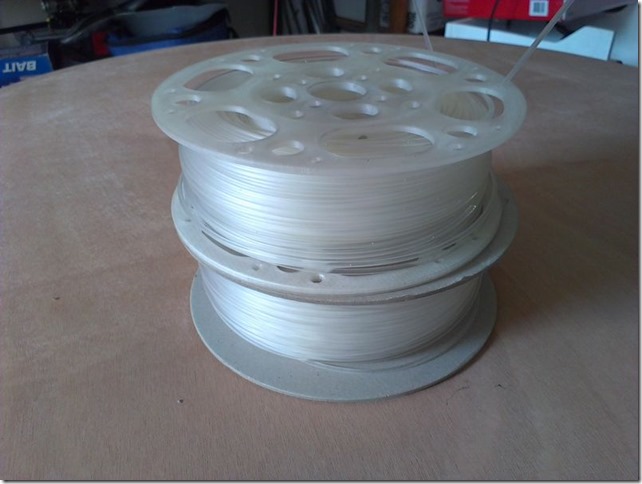
The end result: nice filament. It is not 100% perfect yet, but still very usable. I have printed 5+ kilo of this filament already! You can see the results all over this blog.